
Efficient design automation
A proprietary platform speeds up time-to-market, with a clock architecture built for faster timing convergence.
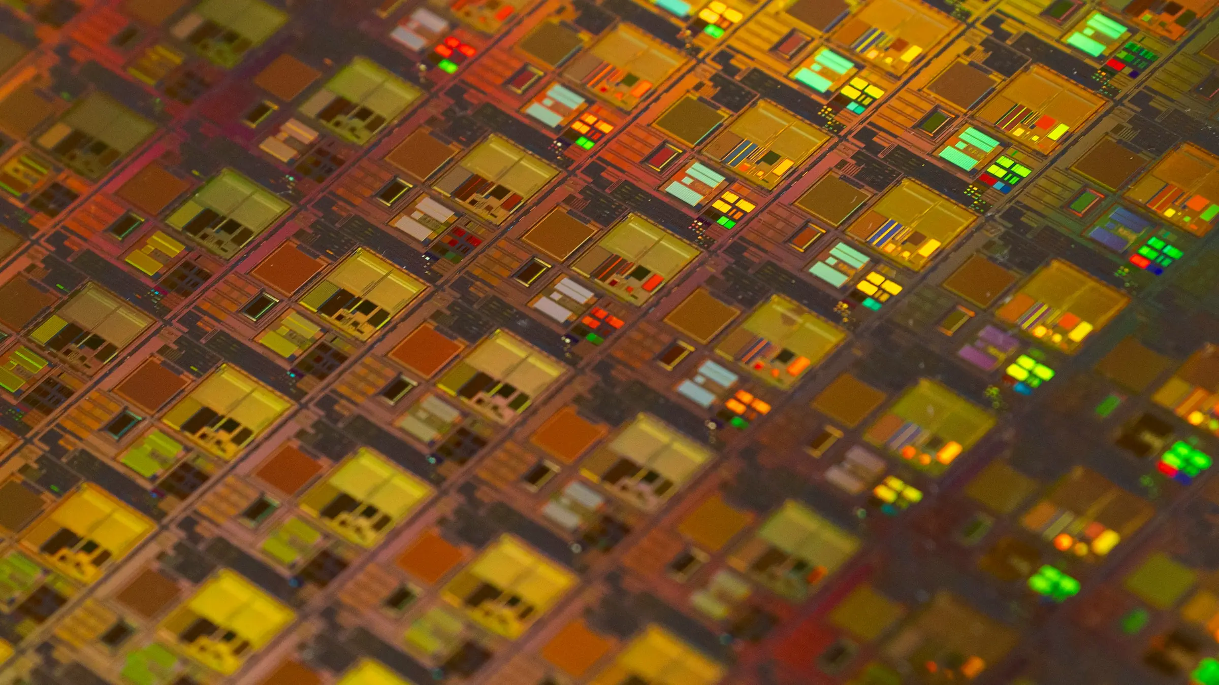
Kern Silicon designs data-center AI accelerators — and provides the design services and IP that get other people's silicon to tape-out.

Kern Silicon works on three fronts: silicon IP, ASIC design services, and our own data-center AI accelerator.
Analog, digital, AFE and high-speed interface IP. Frontend and backend implementation from specification through to tape-out. And a full-size inference chip that proves the platform carries a design all the way to production.
One library, one team. What we learn building our own silicon goes straight into a customer's project.
MoreSpec to RTL, RTL to netlist, netlist to GDSII. Frontend and backend implementation, DFT, system prototyping and software — engaged at whichever stage the project needs, not as an all-or-nothing package.
Physical backend is where most schedules slip, so that is where we are strongest: timing closure, power integrity and sign-off on a proprietary platform, with a clock architecture built for faster convergence.
Spec → RTL → Netlist → GDSII
Analog, digital, AFE and high-speed interface IP, plus the software layer that goes with it. One-stop coverage, so a project does not stall for six months waiting on a third-party block that was supposed to be ready.
Every block is carried into production by our own design team before it reaches a customer — the library and the service arm sharpen each other.
Analog · Digital · AFE · High-speed interface · Software
Our own inference accelerator for LLM and AIGC workloads — a full-size, HBM-class chip on TSMC 6nm, carried through CoWoS packaging to production.
It is a product in its own right, and it is also the proof behind the other two: the IP inside it and the flow that built it are the same ones a customer gets.
TSMC 6nm · ~600 mm² · HBM3e × 4 · CoWoS
Backend is where schedules die. Timing closure, power integrity, sign-off — handled on a proprietary platform with a clock architecture built for faster convergence, so the tape-out date you were given is the tape-out date you get.
A proprietary platform speeds up time-to-market, with a clock architecture built for faster timing convergence.

Close partnerships with leading EDA vendors — their tools integrated into our methodology, with the right flow proposed per application and process node.

Physical design implementation, layout optimization, timing closure and power integrity — one engagement, not four vendors.

Performance and reliability terms set by competitive global markets, whoever the client is.
Built for LLM and AIGC inference: a customized AI core across INT4, INT8, FP8, BF16 and FP16, fed by four HBM3e stacks on a CoWoS package.
One die, two memory builds — capacity-first or cost-first, depending on the deployment.
| Configuration | SKU 1 | SKU 2 |
|---|---|---|
| Stack | 4 × HBM3e | 4 × HBM3e |
| Speed | 8 Gbps | 6.4 Gbps |
| Config | 24 Gb — 12 Hi | 24 Gb — 8 Hi |
| Per stack | 36 GB | 24 GB |
| Total capacity | 144 GB | 96 GB |
Powering your journey to compute excellence.